


Description Of DDR RAM Memories; What Is RAM Frequency, Latency And Timing?
In This Article, We Are Going To Learn More About The Types Of DDR RAM Memories, Their Technical Specifications, And How They Work, And We Will Examine The Different Generations Of These Memories From DDR To DDR4 And Compare Them With Each Other From Various Aspects.
We will also review the technical terms of DDR memory, such as RAM frequency, data transfer rate, delay, and timing.
What are the features of DDR RAM?
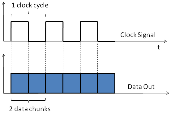
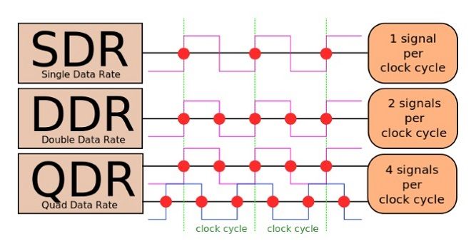
DDR SDRAM memory, or short DDR RAM, is a type of temporary Memory with dynamic random access (SDRAM) that transfers two data units instead of one data unit in each clock cycle, so the entire term of DDR is Double Data Rate or DDR in short. These memories have replaced the old SDR SDRAM memories in which one bit of data was transferred per clock cycle.
In DDR RAMs, one data unit is moved in each rise of the clock, and one unit of data is moved in each fall of the watch; Therefore, the data transfer rate of these memories will be doubled at the same clock speed compared to memories without this feature.
Therefore, the speed label manufacturers put on DDR RAM modules is twice the actual clock speed of that Memory. For example, DDR4-2133 memory works with a clock speed of 1066 MHz, but the manufacturing company declares its clock speed 2133 MHz.
Sometimes the speed listed on the DDR RAM module is also called the adequate speed. In this article, for simplicity, we will contact the speed listed on the DDR memory physical module, the effective speed, and the clock speed with which the Memory works, the actual speed.
Due to the carrying of two bits of data per clock cycle by DDR memories, the manufacturers declare the clock speed twice the actual clock frequency of the module.
Of course, it should be known that the clock speed specified for each DDR memory is the maximum speed of that Memory, and there is no guarantee that the Memory in question will work automatically and stably at that speed.
For example, if we install DDR2-1066 memory on a socket where it is possible to work with a real clock rate of 400 MHz (or 800 MHz DDR), the maximum practical speed achieved for this memory module is 800 MHz.
Because the clock signal is predicted and supplied by the memory controller located inside the processor and outside the module, and this controller has the maximum ability to process data with a clock rate of 400 MHz at the output of the module (generally, DRAM memory controllers are either integrated inside the processor or installed in a chip called the north bridge of the motherboard ).
Considering that 2 bits of data are exchanged in DDR memories in each clock cycle, by multiplying the actual clock speed by 2, the number of transferred data (Transfer) per second is also obtained, which is expressed in the unit of million transfers per second (MT/s), and sometimes this number is declared as an alternative to the effective clock speed of DDR memory.
DDR memory naming method
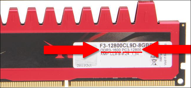
The term DDRx-it is used to name the memory chips in a module, where the letter x indicates the generation of the Memory (such as DDR2 or DDR3), and the number yyyy means the effective clock speed of the desired Memory. But to name the memory modules (DIMM) themselves, the term PCx-Z is used, where the letter x again indicates the generation of DDR memory, and the number expresses that memory module’s maximum data transfer rate.
To calculate the maximum data transfer rate of a memory module, the effective speed of that DDR RAM is multiplied by 64 and then divided by 8 to convert the result into bytes (DDR RAM Bus). In this regard, 64 is the bus width of DIMM memory modules used in personal computers because DIMM modules transfer data in 64-bit packets. With this formula, you can compare the types of DDR ram buses.
In other words, if we multiply the effective clock rate of a DDR memory by eight, that memory module’s maximum data transfer rate is calculated. The total data transfer rate of a module at the interface between the memory controller and the module can be considered the bandwidth of that module.
The maximum data transfer rate of the memory module = the effective speed of the module x 8
For example, if the word DDR3-1333 is written on the memory module, it is from the third generation of DDR memory, and its effective clock speed is 1333 MHz RAM.
Therefore, the maximum data transfer rate of this Memory is obtained by multiplying the number 1333 by the number 8, which will be 10666 megabytes per second, so this memory module is defined as PC3-10666, which is included on the module label along with the name of the memory chip used (DDR3-1333). Sometimes the obtained number is rand; for example, instead of 10666, the memory module is identified as PC3-10600.
It should be noted that the speed and data transfer rate stated on the DDR RAM labels are the maximum speed and data transfer rate of that module, and access to these numbers may not be practically possible due to the limitations of the motherboard.
On the other hand, to calculate these numbers, it is assumed that data is exchanged between the chip and the memory controller in each clock cycle, which usually does not happen; Because in some processes, instead of data transfer, instructions and commands are transferred between the controller and the chip.
For example, sometimes, a command from the controller is sent to the module in some cycles to deliver the data stored in a specific memory location to the controller. No data is transferred between the controller and the chip in such cases.
Comparison of DDR RAM types
Clock speed and data transfer rate of different generations of DDR memory
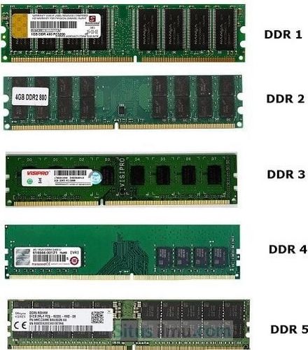
Five generations of DDR memory have been presented, including DDR, DDR2, DDR3, DDR4, and finally DDR5. The main difference between different generations of DDR memory is the maximum data transfer rate achieved in each generation of these chips. For example, the maximum data transfer rate of DDR3 memory equals 12800MB/s, and the maximum data transfer rate of a DDR2 module equals 8533MB/s. Of course, the data transfer rate is only one of the characteristics of DDR ram, and when buying, you should also pay attention to other things, such as the frequency of DDR RAM.
It should be noted that some manufacturers can offer modules with speeds higher than the above standards in each generation of DDR, that these higher speeds can only be achieved through overclocking the module. Usually, the motherboard does not set the output of the memory module to that speed.
For example, suppose you purchase a DDR3-2133 or PC3-17064 memory module and install it into your system’s DDR3 socket. The number 2133 is this module’s maximum effective clock speed, and the clock frequency with which this module works under normal conditions is a smaller number.
DDR3 modules generally work at a standard effective speed of 1333 MHz (actual speed 666 MHz), and to reach an effective rate of 2133 MHz (actual speed 1066 MHz if the motherboard supports it), the RAM must be overclocked manually.
The working voltage of DDR memory
Another difference that DDRx memory has with each other is the working voltage of the memory chips. Generally, with the progress of these chips in higher generations, the working voltage of the memory chips decreases, and the memory chip that works with a lower voltage will eventually get less power consumption.
Usually, DDR chips work with a voltage of 2.5 V, DDR2 chips with a voltage of 1.8 V, and DDR3 chips with a voltage of 1.35 to 1.5 V, and finally, the working voltage of the fourth generation DDR4 chips is only 1.2 V; Therefore, it can be seen that the voltage of each generation is lower than the previous generation. The last column of table number (1) presents the working voltage of each age of DDR RAM.
Prefetch DDR memories
Dynamic memories store data in a matrix of electronic housings or capacitors. In all DDR memories, two data units are exchanged between the buffer and the controller in each clock cycle, but the amount of data transferred from the chip to the pad in each clock cycle is different in different generations; Transferring a certain amount of data from the chip to the memory buffer is called fetch.
The buffer or Memory Buffer Register is a part of the memory module where data is temporarily stored before being transferred to the chip or delivered to the controller, and it is an intermediary between the RAM chips and the central processor. When we talk about the clock speed of a memory module, we mainly mean the external speed of that module, that is, the clock speed at the interface between the module and the memory controller, and the internal clock speed or the clock speed at the output of DDR chips is a fraction of this speed.
The array of DDR chips transfers two data units to the module buffer in each clock cycle; this method is called double-bit fetching. Then in DDR2 memory, the number of data transmitted from the chips to the pad is 4 bits; in DDR3 memory, the number of data transferred to the buffer is 8 bits. In DDR4 memories, despite the higher technology, the number of fetched units is still eight bits.
To adapt the clock speed at the chip output (DDR chip interface and buffer) and the module output (buffer interface and memory controller) and to avoid creating a bottleneck, the actual clock speed at the chip output is set in such a way that by multiplying it by the number of fetched data, the effective clock speed at the buffer output is obtained.
In the figure below, this issue is drawn; In each generation, the DDR (effective) clock speed at the buffer output is calculated by multiplying the actual chip output clock speed by the number of data transferred to the buffer per clock cycle. The actual clock speed at the pad’s output is half that value (the buffer transmits two data units to the controller per clock cycle).
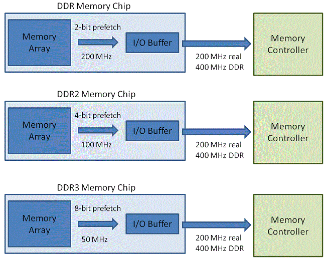
So, according to the figure above, in DDR2 memory, where the clock speed of the DDR RAM at the buffer output is 400 MHz, the clock speed of 100 MHz at the chip output will be sufficient to match the module’s internal and external clock speed. If we have a DDR3-type chip with the output speed of the module at 400 MHz, the chip output clock speed of 50 MHz is sufficient to achieve this match.
According to the above, in all three memory models, DDR2-800, DDR-400, and DDR3-1600, the internal clock speed of the memory module (chip output speed) is set to 200 MHz. Still, the effective output speed of the buffer (at the interface between the module and the controller or xxx value) is 400, 800, and 1600 MHz, respectively.
This is the same method of increasing the clock speed in RAM generation after generation. Table number (1) details the internal clock speed, the number of fetched data, and the number of data transferred to the controller in each clock cycle in different generations of DDR.
Latency of DDR RAMs
The delay in RAM is the time it takes from the request of specific data by the memory controller to the module to the delivery of the desired data through the module to the controller. In other words, the delay of Memory is when the memory controller waits to receive the desired data after the request. The abbreviations CAS or CL also refer to the delay in DDR RAMs.
The delay in RAM is the time it takes from the request of specific data by the memory controller to the module to the delivery of the desired data through the module to the controller.
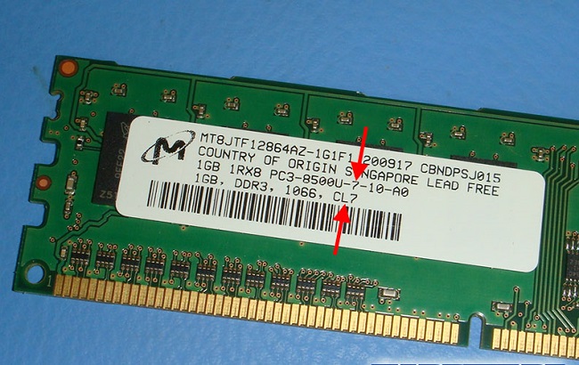
Memory latency is usually expressed in terms of the number of clock cycles. For example, the CL3 memory is a memory in which three clock cycles pass from the time a specific data is requested by the memory controller to the delivery of that data to the controller.
For Memory with CL5 delay, this time is longer and equal to 5 clock cycles. Therefore, the lower the CL delay time, the greater the ability of the memory module and its chips to execute commands received from the controller and retrieve data from the desired row and column in the Memory and deliver it to the controller, and this module works faster. So, to buy memory modules, it is better to look for DDR RAM with less CAS delay.
DDR3 memory has more latency than DDR2 memory, which is even higher for DDR4 memory. For example, the delay in DDR3-1333 memory is equal to 6 clock cycles, and in DDR4-2666 memory is similar to 18 clock cycles.
On the other hand, in each generation of these memories, the memory delay increases as the clock frequency of the module (or RAM frequency in general) increases. For example, in DDR4 memories with a clock frequency of 2133 MHz, the CAS delay is eighteen clock cycles, and if the clock frequency reaches 3200 MHz, the delay will increase to 24 clock cycles.
Although the delay in DDR RAM increases in terms of the number of clock cycles with the advancement of generations, the overall amount of uncertainty will be lower to the increase in the frequency of the module at higher ages and the reduction of the time of each clock cycle, sometimes the amount of memory delay is also expressed in time units; For example, in DDR4-2600 memory, each clock cycle lasts 0.75 nanoseconds (to calculate the time of each clock cycle, the number 1 is divided by the actual clock frequency of the Memory, for example, in the case of the above Memory with an actual clock speed of 1333 MHz, the duration of each clock cycle is equal to 1/1,333,000,000). So, if the delay in this Memory is 18 clock cycles, the delay time is calculated as 13.5 nanoseconds.
By summing up the above, we can say that although the amount of delay increases according to the number of clock cycles as the working frequency of a chip increases, increasing the number of clock cycles does not necessarily mean longer CAS delay or controller waiting time; Because the duration of each clock cycle decreases with increasing memory frequency.
For example, the waiting time for data delivery to the controller (CAS delay) in DDR3-1333 memory with a delay of 6 clock cycles is 13.5 nanoseconds, and for a faster DDR4-2666 memory with a delay of 18 clock cycles, the waiting time for the controller will be the same as 13.5 nanoseconds. Also, DDR2-800 memory with a delay of CL5 has a hold of 12.5 nanoseconds, which is more than the delay of DDR3-1333 memory with CL7 and a delay time of 10.5 nanoseconds.
In general, the delay time is a function of the clock frequency of the memory module; The higher the memory clock frequency (and naturally the RAM frequency), the shorter the data delivery time to the controller.
What is computer RAM timing?
Memory manufacturers usually specify the timing of a memory module with a string of numbers separated by a space. For example, the number strings 5-5-5-5 or 10-10-10-7 are different types of DDR RAM timing.
In this series of numbers, the first number is the CAS delay. These numbers are usually included on the label of DDR RAM modules. At the same clock frequency, the smaller the numbers in this series, the more influential the Memory is.
The only critical parameter for regular users is the type of DDR memories, i.e., DDR3, DDR2, etc. But for professional users and those who expect a higher level of performance from a memory module, other issues, such as memory timing and its delay, cannot be ignored.
If we have two DDR RAM modules with the same data transfer rate but with different timing, the performance level of these two modules will not be the same, Although both run at the same clock speed.
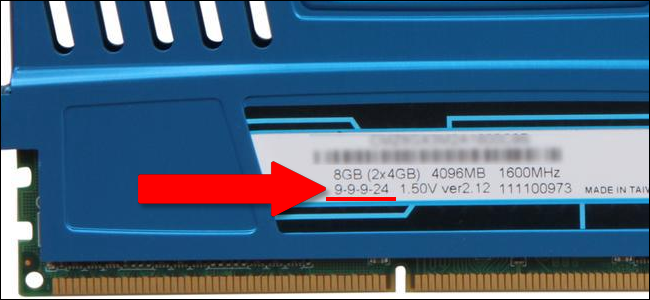
The series of numbers expressed in a memory’s timing tells the Memory’s delay time in doing different tasks. For example, the first number in this series represents the amount of CAS delay.
To understand the meaning of other numbers in this series, we must first know that data is organized in a matrix in DRAM memory chips; That is, the data is stored at the intersection of different rows and columns. The naming of each quantity in the series of timing numbers is as follows:
CL-tRCD-tRp-tRAS-CMD
Each number expresses the time required to do a different task in the Memory, which we will discuss separately in the following.
CL or CAS delay
This number indicates the time it takes from the controller to send a command to the memory chip until the chip responds to that command. This number is the number of clock cycles that elapsed from the request of the processor to receive specific data until the delivery of that data by the chip to the processor, which we explained in detail earlier.
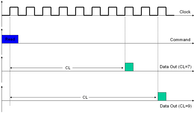
In the above figure, it can be seen that in CL7 memory, from sending the Read command from the controller to read specific data in a part of the Memory until the desired data is delivered to the controller by the module, it took seven clock cycles. This amount for Cl9 memory is equal to 9 clock cycles.
tRCD delay (RAS to CAS delay)
It is the time spent to activate the row and column of the matrix in which the data is stored. Each memory chip is organized internally as a matrix. At the intersection of each row and column, there is an electronic house or a small capacitor that takes the values of 0 and 1 when charged and discharged. The stored data is accessed with the first activation of the corresponding row and column in which zero or one data is placed.
This activation of the desired row and column is achieved with two control signals named RAS, or Row Address Strobe, and CAS, or Column Address Strobe, one after the other. The shorter the interval between sending these two signals, the better the Memory and the faster the data is read.
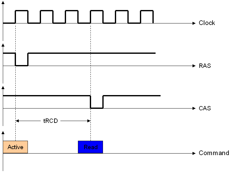
As seen in the above diagram, the RAS to CAS delay can be considered as the number of clock cycles from the issuance of the activation command of an electronic house in the chip to the distribution of the next read or write order; this amount of delay is also based on the actual clock of the memory module, just like the CAS delay. The lower the delay, the faster the Memory and the faster the reading or writing from/to the Memory.
The archtRp (or RAS Precharge)
The time it takes to restrict access to one row of data and enable access to another row of data. In the figure below, this delay is plotted regarding the number of clock cycles.
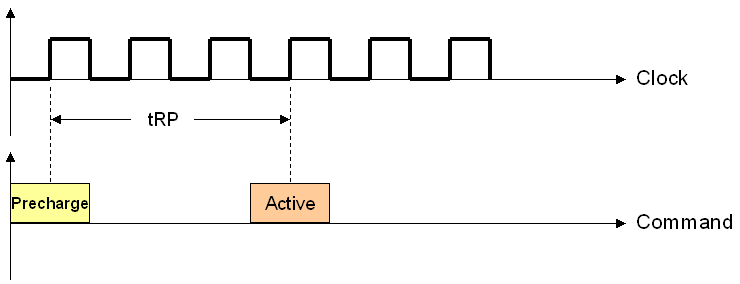
After accessing data from the Memory, it is necessary to issue a command called Precharge. By giving this command, a line of Memory that was recently used is disabled, and another line is activated.
RAS Precharge time is the time it takes from issuing the Precharge command to giving the following activation command. The activation command, as mentioned, leads to reading or writing data from the specified part of the Memory.
This parameter, like CAS and RAS to CAS, works based on the actual clock of the chip and not the clock listed on the memory label. The smaller this parameter is, the faster the DDR memory is and the earlier the following activation command is issued.
Considering the above delay values, the total delay of the module is equal to tRp+tRCD+CL.
tRAS delay
It is the time the processor waits for subsequent access to the Memory. In other words, after issuing the activation command, giving another Precharge command will not be possible until the tRAS time elapses. So this parameter limits the reading or writing of another row of data.
CMD delay
It is the time that elapses from the start of the chip activation until the following command is sent to the Memory. Sometimes, this value is omitted; Because it usually will not exceed two clock cycles. The amount of this parameter is determined by the letter T as 1T meaning one clock cycle or 2T meaning two clock cycles.
The last two parameters, tRAS and CMD, also work with the Memory’s actual clock; the lower the DDR memory, the faster it will work.
Learn more about DDR4 memory.
The fourth and last generation of DRAM used in desktop computers is DDR4. These memories have a higher clock speed and maximum data transfer rate than the previous generations of DDR2 and DDR3.
On the other hand, due to the different physical interfaces of these memories and the lower working voltage level, it is not compatible with memory sockets of previous generations, including DDR3. DDR4 memories officially entered the hardware market in the third quarter of 2014 with the release of Haswell E-series processors, which were optimized to work with DDR4 memories.
The memory density in these new generation chips is higher; While the DIMM memory density in the DDR3 standard was 8 GB (16 4 GB chips); This means that in each module, there is a maximum possibility of accessing 8 GB of RAM, the chip density is higher in the DDR4 standard, and in each module, it is possible to embed up to 16 GB of Memory (16 8 GB chips).
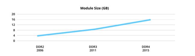
Elite has made efforts to increase the chip density in DDR3 memory; for example, 16 GB modules were produced for enterprise and server applications. However, only AMD processors could support these modules, and Intel processors were limited to 8 GB modules. For this reason, modules higher than 8 GB in the DDR3 standard never became common.
In DDR4 memories, we see an increase in RAM frequency (module set clock frequency), higher data transfer rate, higher chip density, lower voltage consumption, and lower power consumption compared to the DDR3 standard.
The voltage requirements of DDR4 memory are lower than the previous generations, and on the other hand, a higher data transfer rate can be accessed with the new generation modules; As mentioned, the most crucial difference between DDR memory modules of different generations is their data transfer rate.
Although the number of data fetched by the buffer in DDR4 memory has not changed compared to DDR3, by issuing and responding to a more significant number of data read and write commands with a better classification of chips, it is possible to achieve a higher data transfer rate in these memories.
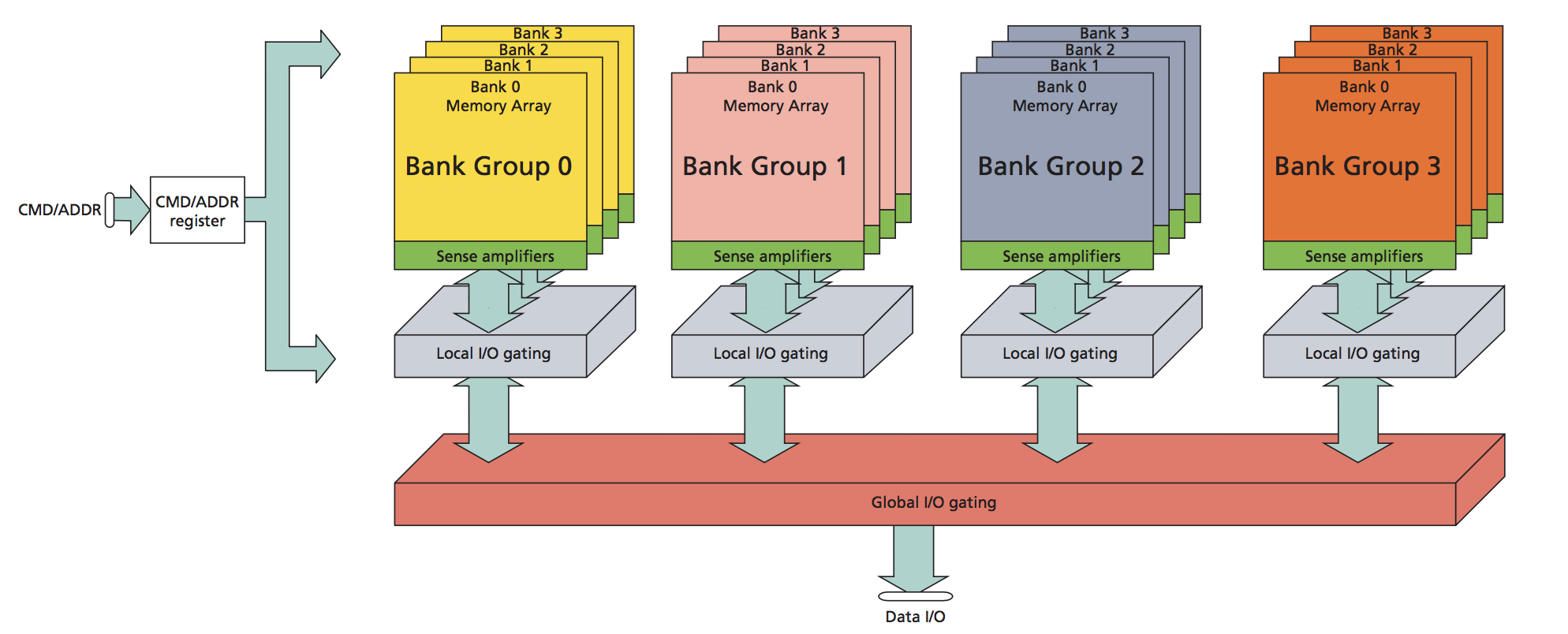
To establish such a mechanism in the DDR4 standard, DRAM chips are divided into four groups of banks, each group consisting of four banks of addressable internal Memory, and thus it is possible to transfer data to each of these groups of different banks (16 banks in total) with more repetition and, of course, faster than before. In DDR3 and DDR2 standards, the chip array consisted of 8 internal banks.
Considering that with the increase in clock speed, the power consumption also increases while reducing the working voltage level of DDR4 chips, it is possible to access higher rates without unreasonable power and cooling requirements.
DDR4 memory operates at a 1.2 to 1.4 V (standard 1.2 V) and an accurate clock frequency of 1066 to 2133 MHz (DDR4-2133 to DDR4-4266). Meanwhile, the previous generation of these memories, DDR3, works with a voltage of 1.35 to 1.5 volts and a fundamental frequency range of 400 to 1067 MHz.
Admirable foresight is considered in the fourth generation of DDR RAM. The DDR4 standard is the first memory standard in which the possibility of 3D stacking of DRAM chips is foreseen. In this method, it is possible to accumulate eight slave chips on one master chip, which can be addressed independently through the master chip.
The last point about DDR4 memories is that with the increase in chip density and the possibility of planting smaller ICs but with more capacity than the DDR3 standard, the cost of production will be reduced, and, as a result, the price level will be more reasonable. For example, to create a capacity of 8 GB in a DDR3 module, it is necessary to install 16 4 GB chips in it, while in the new standard, the same amount of capacity can be achieved by planting 8 8 GB chips in a smaller space.
How to identify different types of DDR RAM?
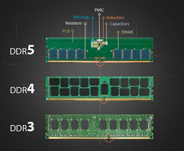
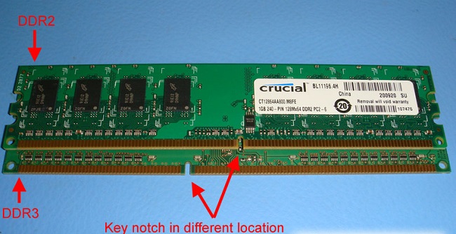
DDR RAM modules are also physically different. Memory modules are electronic boards to which DRAM chips are attached. These modules have several pins at the bottom, connecting the module to the motherboard resources. DDR2 and DDR3 memories are each connected to the motherboard socket with 240 pins, and only the notch in the module is different.
In DDR4 memory, the number of module pins is 288, and the location of the notch is also different from DDR3. Therefore, it is not possible to install DDR4 memories on DDR3 sockets.
DDR2 memories connect DRAM chips to the electronic board by soldering (Ball Grid). But in the first-generation DDR memories, this connection was established through the sinking bases in the panel.
Due to the physical differences between different generations of DDR RAM, using the same Memory on an older memory socket is impossible. Therefore it will be necessary to upgrade the motherboard and possibly the processor to use newer Memory.
What is the maximum DDR ram that can be supported on my computer and laptop?
One common question new computer users face is the ability to detect the maximum amount of RAM installed on the system. For this, you must execute the following command in Command Prompt or CMD in the Windows operating system.
First, open the system’s Start menu and then type CMD. Click on Command Prompt to open its black screen. In the next step, copy the command code below and enter it in the Command Prompt.
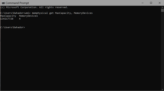
The number displayed in this section shows the amount of RAM that can be supported in kilobytes. To convert this number to gigabytes, you need to divide it by 1048576. For example, the number obtained for the Hardware City test system is 128 GB; the computer can support up to 128 GB of RAM.
Frequently Asked Questions
In this section, frequently asked questions about RAM are addressed.
What is RAM frequency?
RAM frequency indicates how often data is written to and read from RAM, measured in megahertz. This feature is directly related to the speed and performance of RAM.
What is megahertz RAM?
Megahertz measures RAM frequency, and each megahertz means one million cycles per second.
What is DDR in a graphics card?
DDR stands for Double Data Rate or double data rate memory used for RAMs. In graphics cards, GDDR or graphics memory with double data rate is used, which was introduced as an alternative to SDR, which transfers two bits per clock pulse and is twice as fast as the previous generation models.
How to find out how much ddr motherboard is?
There are different ways to do this. The easiest way is to use the Windows Task Manager, executed using the combination keys Ctrl+Alt+Del. After opening the Task Manager, go to the Performance tab and click Memory. In this section, the DDR type of system RAMs is specified. The following method uses utility software such as CPU -Z, which can be found in the memory section, where all the specifications of the system RAMs can be found. In this software, you can learn about the DDR of the motherboard by referring to the Memory tab and reading the information in front of the Type section.