


Everything We Know About Nvidia’s Ada Lovelace Architecture And RTX 4000 Graphics
Nvidia Claims That The Company’s Next-Generation Graphics Card, The RTX 4000 With Ada Lovelace Architecture, Will Be Unrivaled in Performance And Power Consumption.
There are a lot of rumors right now about Nvidia’s plans for Ada Lovelace architecture; Nvidia’s RTX 4000 graphics cards with Ada Lovelace architecture are scheduled to be available by the end of 2022, two years after the Green Team Ampere architecture, and possibly between September and October (September and October 1401). Nvidia calls the architecture of these graphics in honor of the famous mathematician and the first programmer in history, Ada Lovelace.
In early March 1400, a group of hackers attacked Nvidia’s servers, leaking a significant amount of information about the company’s GPUs. Stay tuned to see everything we know about Nvidia’s Ada Lovelace architecture and the RTX 40 family.
In early April, the Green team introduced its Hopper H100 data center GPUs in detail.
Hopper architecture and the H100 GPU should not be confused with the Ada architecture.
The Hopper H100 will replace the Ampere A100, a replacement for the Volta V100. Examining Nvidia’s product offering, it is expected that its other consumer products, such as graphics cards, will be available in the future.
For example, the A100 GPU was officially introduced in May 2020, and the Ampere GPUs in the form of the RTX 3080 and RTX 3090 graphics cards about four months later. If Nvidia pursues a similar program to release GPUs based on the Ada Lovelace architecture, RTX 40 graphics cards will likely be available at the same time between August and September.
GPU |
AD102 |
AD103 |
AD104 |
AD106 |
AD107 |
|---|---|---|---|---|---|
| The manufacturing process | TSMC 4N | TSMC 4N | TSMC 4N | TSMC 4N | TSMC 4N |
| Number of transistors | Probably 60 billion | Probably 40 billion | Probably 30 billion | Probably 20 billion | Probably 15 billion |
| Computational units | 144 | 84 | 60 | 36 | 24 |
| Number of CUDA cores | 18.432 | 10.752 | 7.680 | 4.608 | 3.072 |
| Number of tensor cores | 576 | 336 | 240 | 144 | 96 |
| Number of RT cores | 144 | 84 | 60 | 36 | 24 |
| Turbo frequency | 1.6 to 2.0 GHz | 1.6 to 2.0 GHz | 1.6 to 2.0 GHz | 1.6 to 2.0 GHz | 1.6 to 2.0 GHz |
| L2 cache (MB) | 96 | 64 | 48 | 32 | 32 |
| VRAM speed (Gbps) | 21 to 24 | 21 to 24 | 16 to 21 | 16 to 21 | 14 to 21 |
| Video memory bus width (bits) | 384 | 256 | 192 | 128 | 128 |
| Render Output Unit (ROP) | Probably between 128 and 196 | Probably 112 | Probably 96 | Probably 64 | Probably 48 |
| Texture Mapping Unit (TMU) | 576 | 336 | 240 | 144 | 96 |
| Power to perform single floating-point calculations (FP32) | 59 to 73.7 teraflops | 34.4 to 43 teraflops | 24.6 to 30.7 teraflops | 14.7 to 18.4 teraflops | 9.8 to 12.3 teraflops |
| Power of 16-bit half-precision calculations (FP16) | 472 to 590 teraflops | 275 to 344 teraflops | 197 to 246 teraflops | 118 to 147 teraflops | 79 to 98 teraflops |
| Bandwidth (Gbps) | 1008 to 1152 | 672 to 768 | 384 to 504 | 256 to 336 | 224 to 336 |
| Thermal design power | Less than 600 watts | Less than 450 watts | Less than 300 watts | Less than 225 watts | Less than 150 watts |
| Rough price | More than a thousand dollars | Between $ 600 and $ 1,000 | Between $ 450 and $ 600 | Between $ 300 and $ 450 | Between $ 200 and $ 300 |
Rumored specifications of Ada graphic processors
Estimates for Ada GPU frequency in the following article are in line with previous Turing and Ampere architectures and range from 1.6 to 2.0 GHz. However, Nvidia is likely to offer frequencies beyond this value for this generation of processors. Graphics, for now, we will suffice with a conservative estimate.
Another premise considered in the present article is the custom TSMC 4N process (or 4nm process) in all Ada GPUs.
The Hopper H100 GPU is manufactured with the 4N TSMC process; The process appears to be a modified N5 TSMC process that is widely used in the chips of Apple iPhones and laptops and is rumored to be the same process for GPUs based on Ada Nvidia, RD-based Zen 4 processors and GNA processors. Three is also used; It should be noted that today the name of process nodes (nanometer number) is no longer related to the physical properties of chips, and the physical scale of chips is only considered as symbols for marketing.
The number of transistors is the best criterion for judging each chip.
We know that the Hopper H100 GPU will have about 80 billion transistors, and the A100 GPU will have twice as many GA102s as 56 billion transistors. According to some reports, Nvidia intends to increase the number of transistors in the AD102 GPU by double the number of H100 transistors.
Based on the information leaked so far, and at least on paper, the Ada architecture seems to have an awe-inspiring performance. In Ada architecture, the number of computing units (SMs) or Streaming Multiprocessors and their cores is much higher than current Ampere GPUs, which alone can significantly increase performance.
Streaming Multiprocessors (SMs) are part of Nvidia GPUs used to calculate operations.
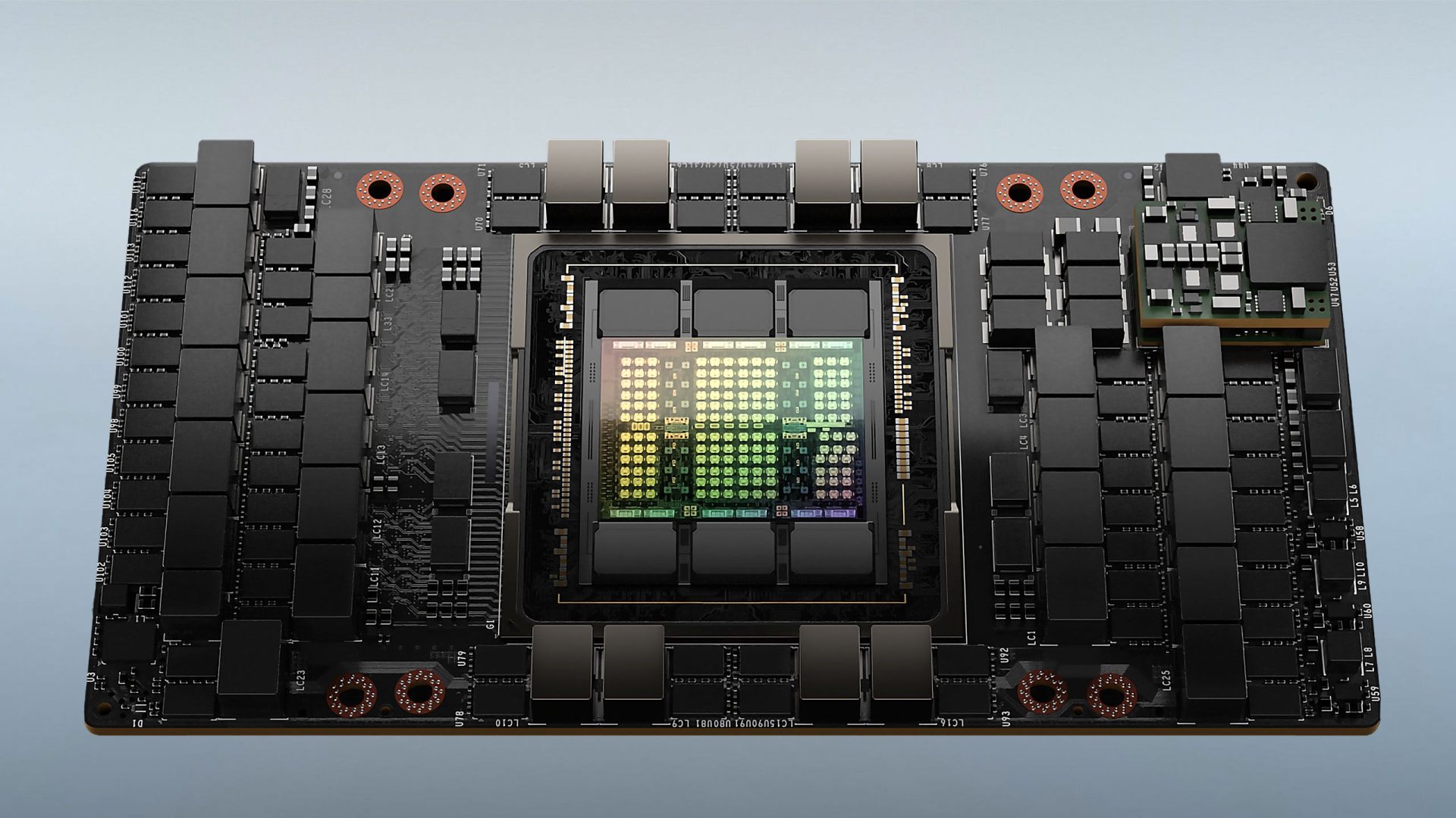
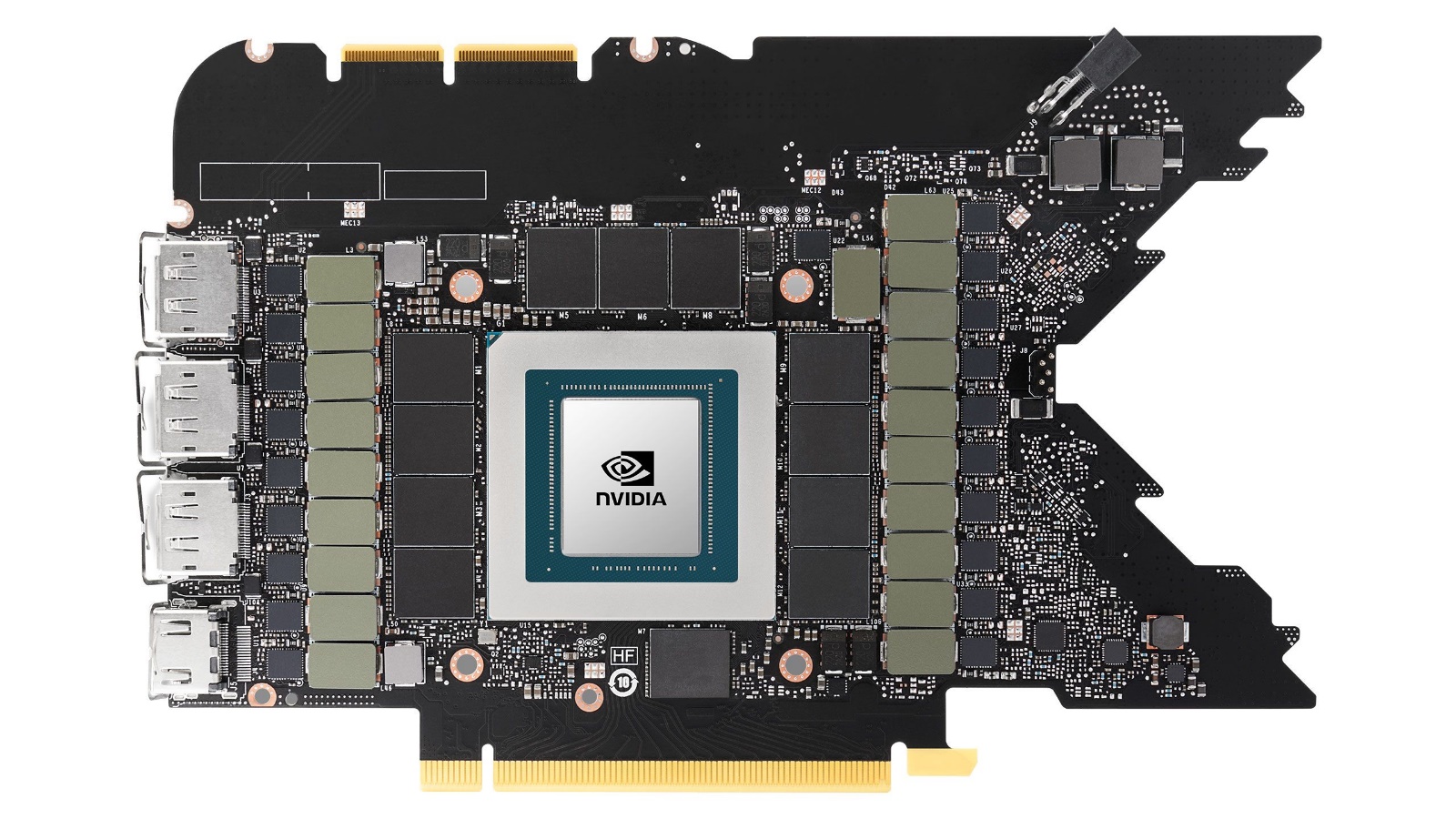
Examining the Hopper H100 GPU reveals details about the Ada architecture
Even if the specifications of the Ada architecture are weaker than what was leaked, we can still be sure that this architecture will perform better for next-generation GPUs. The RTX 4090 is a significant improvement over the RTX 3090 Ti. will be.
The RTX 3080 was about 30 percent faster at launch, and the RTX 3090 was 45 percent faster than the RTX 2080 Ti. So keep in mind that if you are using a regular processor such as the Core i9-12900Kor Ryzen 7 5800X3D, you will need to upgrade your system processor to get the most out of all the power and speed of Ada GPUs.
Significant increase in computational performance in Ada architecture
We will first introduce the types of cores available in Nvidia’s RTX series GPUs.
- The first type is the CUDA cores used for general computing; Thousands of these cores are placed parallel on modern GPUs and are responsible for shading each pixel and all other graphic effects.
- Next, RTX cards have cores called tensors that perform other computations, such as machine learning and artificial intelligence. These cores can use to accelerate machine learning software in any field, but they also play an essential role in graphics. Nvidia uses tensor cores to enhance beam intercept images and intelligently sample lower-resolution images using DLSS (Super Deep Learning Sampling) technology.
- Finally, we get to the RT cores, which are tasked with performing beam-type calculations as quickly as possible to display a moving image on a screen with a playable frame rate. RT cores, in particular, accelerate the essential mathematics needed to capture virtual beams of light in a snap.
The most crucial change in Ada GPUs will be the increase in computing units (SMEs) in the CUDA cores compared to the current Ampere GPUs. The AD102 GPU has 71% more computing units (SMs) than the GA102 GPU in the best possible conditions. Even if we ignore all the other improvements in this architecture, only this increase in computing power (SMEs) can significantly improve the performance of next-generation GPUs. Be considered next.
Increasing the number of computing units will be effective for visual performance and other areas.
For example, the Ampere architecture calculations on the tensor core and a fully active AD102 chip at a frequency of nearly 2 GHz can increase the power of deep learning computing or AI computing to 590 teraflops in 16-bit half-precision computation (FP16). (Tensor cores are one of Nvidia’s innovations in graphics processing that are widely used in deep learning and neural networks).

For comparison, the GA102 GPU on the RTX 3090 Ti achieves 321 teraflops at best in half-precision calculations; An 84% increase in computing power based on core and frequency counts is likely to apply beam tracking hardware as well. These percentages can be accurate if Nvidia does not change the RT and tensor cores.
According to some reports, extensive changes to the tensor cores are unnecessary, and deep-learning hardware improvements apply more to the Hopper H100 GPU than to the Ada2 ADA-based graphics.
On the other hand, modifications may make to RT cores that increase their performance by 25 to 50% compared to the Ampere architecture, Just like the 75% performance improvement of the Ampere architecture RT cores applied to the Turing architecture.
In the worst-case scenario, just using 4N TSMC lithography (or even 5N TSMC) instead of Samsung 8N lithography, adding more cores, and maintaining the same frequencies can significantly increase the performance of next-generation GPUs; While Nvidia may not be content with this minimal change, even with those changes, the AD107’s low-end GPU will be 30 percent or better than the current RTX 3050.
Remember that the number of units mentioned is for whole chips, and Nvidia will most likely use semi-active chips to improve performance.
For example, the Hopper H100 GPU has 144 units of computing, but only 132 of these are active in the SXM5 version; We will probably see the same approach in the AD102 graphics processor (RTX 4090 graphics card); This means that the number of active computing units for the AD102 will be between 132 and 140, and in lower versions, it will be less. By doing so, Nvidia can make the future graphics card (RTX 4090 Ti) more efficient by fully activating all computing units.
Speculation about the rendering output unit in the Ada architecture
The Render OutPut unit, often referred to as ROP, are a piece of hardware in GPUs and one of the final steps in the graphics card rendering process. ROPs perform transactions between buffers or writing, reading, and combining them in local memory. With the help of their hardware, they make the output images more beautifully displayed with minimal artificial complexity.
Not much is currently known about the rendering output units (ROPs) of Ada GPUs, but we know that in the Ampere architecture, the rendering output units depend on the GPCs; the Graphics processing cluster (GPC) which is a dedicated hardware block for computing, shading and texturing; It consists of four tissue processing (TPC) clusters, each with an unknown number of computational units (SMs) and a raster engine; Even if we know the number of computing units, it is still not clear how many SMs each GPU will have.
For example, if we take the total number of AD102 computing units as 144 units, we will have 12 GPUs, each with 12 computing units; If we assume the number of graphic processing clusters to be eight units, we will have 18 computational units, and if we believe this number to be nine units, we will have 16 computational units. Of course, there are other combinations for the number of GPUs and computing units, but these three combinations seem more likely than all the different modes.
Since the Hopper H100 GPU has eight GPUs with 18 computing units, Ignoring HBM3 memory, this configuration may be even more sensible for the AD102.
Skeptical rumors about the number of computing units in the Ada architecture
The 144 computing units (SMEs) for the AD102 seem a bit dubious; The GA100 GPU had a maximum of 120 computing units, and the Hopper H100 chip had about 20% more than that, 144 computing units, of which 132 are active at best. On the other hand, some rumors suggest that the AD102 GPU has about 71% more computing units than the GA102; Therefore, it seems unlikely that the number of Ada and Hopper computing units will be equal.
The mere citation of data leaked from Nvidia can not confirm the accuracy of the above conjecture. Perhaps it would have been better for Nvidia to offer its new architecture by setting higher frequencies and fewer computing units, like the Red Team’s invention and RDNA2 architecture, but doing so required a more fundamental overhaul.
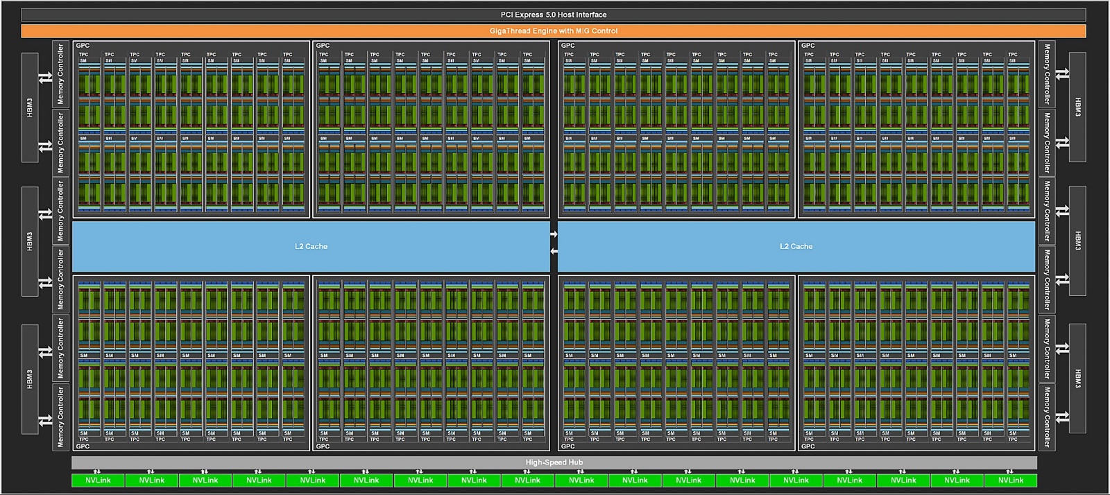 The Hopper H100 GPU is equipped with 144 computing units and has 8 GPUs. Replace HBM3 in this GPU with GDDR6X, change most of the FP64 cores (with double-precision decimal computing power) to tensor cores, then add RT cores; Now, in theory, you might want to consider an ADA2 GPU based on the Ada architecture.
On the other hand, there is a compelling reason for the AD102 chip being large: the presence of beam intercept hardware.
As we know, Nvidia does not make utterly separate silicone for both consumers and professionals. For example, the Green team in the 3090Ti uses the same GA102 chip as in the RTX 3080 and a bit of extra driver functionality.
Although beam tracking is not an essential feature for everyday tasks, it plays an indispensable role for gamers, and the presence of RT cores can be a great boon for them; However, the Hopper H100 GPU, like the GA100, is not equipped with hardware for beam tracking.
In addition, different versions of Ada GPUs will use for platforms that perform AI and machine learning algorithms. So it is likely that there will be a large number of tensor cores in these GPUs.
The 144 computing units for the Ada architecture do not seem far-fetched.
Memory subsystem: Possibility to use GDDR6X in Ada architecture
GDDR6X memory is a high-bandwidth, dynamic synchronous access memory that is approximately twice the data rate produced by Micron. This memory uses multilevel signaling techniques, and according to Micron, its only manufacturer, it can achieve high bandwidth per chip.
Micron recently announced that it intends to provide access to 24 Gbps of GDDR6X memory. The memory speed for the RTX 3090 Ti graphics was 21 Gbps, and since Nvidia uses GDDR6X for all of its products, the new memory speed seems to be related to Nvidia’s Ada architecture; Nvidia’s lower-end GPUs, with a maximum memory speed of 18 Gbps, use regular GDDR6 memory instead of GDDR6X memory.
The Ampere GA102 GPU supports twelve 32-bit memory interfaces with GDDR6X; The AD102 is expected to use a similar layout in addition to faster memory.
This increase in memory speed can be problematic, as GPUs usually have to combine two computing factors and bandwidth to deliver the promised performance. RTX 3090 Ti graphics, for example, perform about 12% more computing and 8% more bandwidth than the 3090.
If the above computational estimates are correct, the RTX 4090 will hypothetically have about 80% more computations than the RTX 3090 Ti, while the bandwidth will increase by only 14%; Such a disproportion causes the count and bandwidth be disconnected.
Increase the GPU. Currently, RTX 3050 to RTX 3070 graphics all use standard GDDR6 memory at 14 to 15 Gbps, and since this standard memory can use at speeds up to 18 Gbps, it can also use for the AdaX architecture at 40 g / s. Nvidia low-end processors have the potential to increase bandwidth assuming GDDR6X power consumption control, so if Nvidia still needed more bandwidth, it could use upgraded GDDR6X memory for lower-end GPUs.
It is unlikely that Ada-enhanced GPUs will come with GDDR7 or perhaps Samsung GDDR6 + at 27 Gbps, but given that no information is yet available on GDDR7 or GDDR6 + memory, we do not see that at this time.
Notable L2 cache usage
One of the best ways to reduce the need for high bandwidth is to increase the cache on the chip. Using the cache system helps the GPU find the next bit of information it needs immediately after the search; This condition is called Cache Hit. More cache will increase the Cache Hit so that the GPU will no longer need to retrieve data from GDDR6 or GDDR6X memory. AMD’s Infinity Cache similarly allows RDNA 2 chips to perform more tasks with less bandwidth. Now leaked information from Nvidia’s Ada architecture and L2 cache indicates that the green team intends to take a similar approach to the red team.
Introduction The Navi 21 GPU uses L3 to 128MB of cache memory. This memory is 96 MB in Navi 22 GPU, 32 MB in Navi 23, and 16 MB in Navi 24. Even the smallest L3 cache capacity among these four capacities works well for the memory subsystem.
Less capacity L2 cache can compete with larger but slower capacity L3 store.
For example, the Radeon RX 6500 XT was not expected to be a powerful graphics card with a Navi 24 GPU, but this low-end product, with 16MB of L3 cache, could compete with graphics cards almost twice the memory bandwidth.
According to published reports, in the Ada architecture, each 32-bit memory controller comes with an 8MB L2 cache; This way, graphics cards with a 128-bit memory interface will have 32MB of L2 cache, and graphics cards with a 384-bit memory interface will have 96MB of L2 cache. Of course, since these values are less than infinity caches, their performance delays can not predict.
L2 cache is slower than the L3 cache, so a slightly smaller capacity L2 cache can compete with a larger but slower L3 stock.
For example, the RX 6700 XT performs about 35% more computations than its predecessor, the RX 5700 XT. On the other hand, Benchmarks show that the GPU also performs approximately 32% better at 1440p Ultra resolution, and overall performance is almost consistent with improved computing.
It should note that the 6700 XT graphics are equipped with a 192-bit memory interface and only 384 GB / s of bandwidth, which is about 14% less than the 448 GB / s of bandwidth of the RX 5700 XT. Therefore, it can conclude that Infiniti C3 L3 brings a 50% increase inadequate bandwidth.
Assuming Nvidia can deliver similar results with the Ada architecture, the 14% increase in bandwidth provided by 24 Gbps of memory combined with a 50% increase inadequate bandwidth will result in the AD102 delivering approximately 71% more effective bandwidth.
Nvidia has shared a lot of details about the Hopper H100 GPU and confirmed the larger capacity of the L2 cache than the previous generation GA100, but this product no longer has 8 MB of L2 cache per memory interface. . In fact, the total L2 Hopper H100 cache is up to 50MB; This amount was 40 MB in the A100. Hopper also uses HBM3 memory and has 80 GB of graphics memory.
Power consumption in Ada architecture
Power consumption in Ada architecture will probably surprise everyone. The first rumors about Ada Architecture’s power consumption were 600 watts; At that time, it was strange for all users to believe this amount of consumption.
For many years, the power consumption of Nvidia graphics cards was close to 250 watts; In the Ampere architecture, this value was increased to 350 watts on the RTX 3090 (and later on the RTX 3080 Ti), which seemed too much. When Nvidia announced the specs of the Hopper H100 GPU and the RTX 3090 Ti graphics card, the belief in 600 watts of power consumption was no longer so far-fetched.
The RTX 3090 Ti currently consumes 500 watts or more of power.
Dennard scale or MOSFET scale (MOSFET) is a scaling law that roughly states that as the transistors get smaller, their power density remains constant. The power consumption is proportional to the area of the transistors. Moore’s Law also states that the number of components of each integrated circuit will regularly double over a predictable period; This period was initially considered 12 months but later expanded to 24 months.
The Denard (or MOSFET) scale shows that each generation can reduce the dimensions by about 30%. With this reduction in sizes, the total area is reduced by up to 50%, the voltage by up to 30%, and the delay in the circuit by 30%.
In addition, the frequencies increase by about 40%, and the overall power consumption is halved; These changes may seem too good on paper, but the fact is that they violated the Denard scale 15 years ago in 2007.
The same is true of Moore’s law; although Moore’s law has not been wholly violated, there are stark differences between the achievements and the law.
From 2004 to date, the maximum frequency of integrated circuits has increased from 3.7 GHz to 5.5 GHz in the Core i9-12900KS, which is approximately a 50% increase over six generations of lithographic improvements. In other words, if it had not violated the Denard scale, today’s processors would have reached a frequency of up to 28 GHz.
It is not limited to frequency, and power and voltage also change on this scale. Today, new lithographs can improve transistor density, but it is also necessary to balance voltages and frequencies.
Nvidia had two approaches:
- The Production of a double-speed chip costs almost twice as much as electricity.
- Produce a chip with more efficient electrical consumption that has a lower speed.
According to published reports, Nvidia seems to have chosen the first approach in Ada architecture:
If you use a 350-watt Ampere GPU like the GA102 and increase performance by 70 to 80 percent, you will consume 70 to 80 percent more power. Now suppose this 350 watts is between 595 and 630 watts; Of course, it is likely that Nvidia will do its best to minimize power consumption, and the 600-watt power consumption is rumored to be the maximum power consumption on reference cards.
Graphics card registration based on Ada architecture
Given the company’s green team naming pattern and investment in the RTX brand, predicting the RTX 40 name for the next generation of Nvidia graphics makes perfect sense. However, still, Ada-based graphics cards may offer different naming.
Ultimately, these products, whatever their name, offer the same powerful performance and impressive capabilities that can surprise users.
Pricing of graphics cards based on Ada architecture
The fact is that Nvidia, like any other brand, wants to monetize its next-generation graphics cards as far as the market is concerned. When launching graphics cards based on the Ampere architecture, the company considered a pricing model that later proved utterly wrong during the Quaid epidemic.
Real-world prices soared, and scalpers made a profit; The involvement of digital currency miners exacerbated this situation, and prices rose again. These graphics cards are currently sold in the market for almost 30% more expensive than Nvidia.

The price of Ada-based graphics cards is likely to rise again. Increasing L2 cache and relatively limited memory bandwidth in Ada architecture increases mining performance compared to Ampere architecture.
Graphics cards based on RDNA 2 architecture are also slightly faster than RDNA-based models, which means that mining alone cannot be the reason for the rise in prices.
Depending on the supply and demand at the time of the Ada graphics card launch, the flagship version of the AD102 may be available for a starting price of $ 999 (possibly for the RTX 4080) and the more powerful model (possibly the RTX 4090) for more than $ 1. The RTX 3090 Ti will sell for $ 999.
Nvidia is even likely to revive the Titan brand for Ada.
We will be. There’s a reason why Nvidia should immediately switch the architecture of all its graphics products from Ampere to Ada. Since no other processor or GPU wants to use Samsung’s Fonderi 8N process, it will likely continue to introduce more RTX 30 GPUs for a long time.
Nvidia is likely to make more money by introducing Ada’s advanced graphics cards and using all the capacity from TSMC. Doing so may even reduce the price of existing RTX 30 series graphics cards.
Pricing information is usually one of the last factors to be leaked about any product; Therefore, at this time, the pricing model of these products can not predict with certainty.
Changes in the design of the Founders Edition Ada graphics cards
When Nvidia introduced the RTX 3080 and RTX 3090 graphics, it made many claims about the design of the Founders Edition of these two products. The Founders Edition version of these two products performs well, but experience over the past 18 months has shown that some third-party cards have a better cooling system and work quieter. The Founders Edition RTX 3080 Ti is a clear example that fan temperature and speed can not be compatible with high-temperature GPUs.
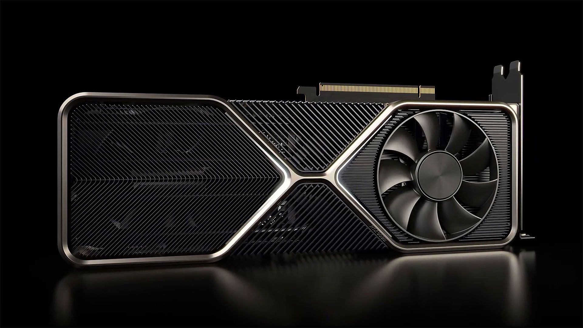
Nvidia RTX 3080 graphics; Different from all previous graphics cards
Given the rumored power consumption of the Ada architecture and its doubling of the Ampere architecture, the Green Team is unlikely to stick to its current industrial design. There is no word yet on Nvidia’s Founders Edition design for Ada graphics. Still, since all graphics cards occupy three or more slots, the company must consider external cooling to eliminate the 600-watt heat.
Release time of Ada GPUs
So far, September to October has been mentioned several times to release Ada GPUs and RTX 40 series. Still, it should remember that the first Ada graphics cards to be introduced will be just the beginning of the release of this series of graphics cards. Nvidia released two RTX 3080 and RTX 3090 graphics in September 2020, the RTX 3070 a month later, and the RTX 3060 Ti a month later.
Green Team RTX 3060 graphics with RTX 3080 Ti and RTX 3070 Ti graphics in June 2021 (June 1400), affordable RTX 3050 pictures in January 2022 (December 1400), and finally RTX 3090 Ti by the end of March 2022 (April 1401) کرد.
Ada graphics cards, similar to Amepere graphics cards, are expected to start with the fastest models and continue with the sale of flagship models.
We’ll probably have an update to Ada graphics almost a year after the initial release, but it’s unclear what these updates will be called (Ti or Super).
More competition in GPU space
Nvidia has been one of the leading brands in the graphics card industry for decades; The Green team controls approximately 80 to 90 percent of the total graphics market and has primarily worked to create and adopt new technologies such as beam interception and DLSS.
However, as artificial intelligence and computing become increasingly important for scientific research and other computing work and rely on processors similar to GPUs, other companies such as Intel have recently entered the field.
Intel did not produce proprietary graphics cards for a long time in the late 1990s and seemed to focus more on media capabilities. The company’s top-of-the-line graphics models, at best, had the power to perform single-float point calculations equal to 18 teraflops, which, according to the table at the beginning of the article, can only be considered a competitor to the AD106 processor.
However, according to published reports, Intel plans to re-enter the field soon, introducing the second generation of Arc Alchemist architecture, called the Battlemage, doubling Alchemist capabilities and taking over Nvidia’s market share, especially in the gaming laptop space.
Ayamdi, for his part, is working to gain a foothold in the industry and has made several statements about his plan to introduce the RDNA 3 architecture by the end of this year.
The red team is expected to use the TSMC N5 node in its next generation of architecture and be able to compete directly with Nvidia in the field of wafers.
The company has so far avoided putting any deep-learning hardware in its consumer GPUs, but given that Intel uses Xe Matrix cores in the Arc architecture, it is likely that Emedi will change its approach; Xe Matrix cores are equipped with XeSS technology that provides capabilities to improve virtual intelligence.
Finally, there is no doubt that Nvidia is currently offering far more impressive beam performance than the RX 6000 series cards; The red team has yet to say anything about beam interceptor hardware or the need for its effects in gaming, and Intel, in turn, may offer poorer beam interception performance than expected.
It is not easy to persuade people to upgrade their graphics cards as long as most games run fast and do not require beam effects. Still, it is to be hoped that after two years of shortages and high prices for GPUs and flagship GPUs, these problems will finally resolve next year, and the GPU industry will once again become a significant industry.